1 同济大学物理科学与工程学院精密光学工程技术研究所,上海 200092
2 上海大学理学院,上海 200444
3 中国科学技术大学国家同步辐射实验室,安徽 合肥 230029
Mo/Si多层膜是13.5 nm极紫外波段理想的反射镜膜系,它与极紫外光源的结合使得极紫外光刻成为了目前最先进的制造手段之一。极紫外光源的实际应用对Mo/Si多层膜提出了高反射率、高热稳定性、抗辐照损伤、大口径等诸多要求。针对极紫外光源用Mo/Si多层膜面临的膜厚梯度控制和高温环境问题,利用掩模板辅助法对大口径曲面基底上不同位置处的多层膜膜厚进行修正;选择C作为扩散阻隔层材料,对磁控溅射法制备的Mo/Si、Mo/Si/C和Mo/C/Si/C三种多层膜在300 ℃高温应用环境下的热稳定性展开了研究。研究结果表明:通过掩模板辅助的方式能够将300 mm口径曲面基底上不同位置处的Mo/Si多层膜膜厚控制在预期厚度的±0.45%以内,基底上不同位置处Mo/Si多层膜的膜层结构和表面粗糙度基本相同;引入C扩散阻隔层后,经过300 ℃退火,Mo/Si多层膜的反射率损失从9.0%减少为1.8%,说明C的引入能够有效减少高温对多层膜微结构的破坏和对光学性能的影响,提高了多层膜的热稳定性。
激光光学 极紫外光源 Mo/Si多层膜 磁控溅射 膜厚控制 热稳定性

Siyi Huang 1,2,3Masao Ikeda 2,3,*Minglong Zhang 1,2,3Jianjun Zhu 2,3Jianping Liu 1,2,3,**
Author Affiliations
Abstract
1 School of Nano-Tech and Nano-Bionics, University of Science and Technology of China, Hefei 230026, China
2 Suzhou Institute of Nano-Tech and Nano-Bionics, Chinese Academy of Sciences, Suzhou 215123, China
3 Key Laboratory of Nanodevices and Applications, Chinese Academy of Sciences, Suzhou 215123, China
A suitable contacting scheme for p-(Al)GaN facilitating quick feedback and accurate measurements is proposed in this study. 22 nm p+-GaN followed by 2 nm p-In0.2Ga0.8N was grown on p-type layers by metal-organic chemical vapor deposition. Samples were then cut into squares after annealing and contact electrodes using In balls were put at the corners of the squares. Good linearity between all the electrodes was confirmed inI–V curves during Hall measurements even with In metal. Serval samples taken from the same wafer showed small standard deviation of ~ 4% for resistivity, Hall mobility and hole concentration. The influence of contact layer on the electrical characteristics of bulk p-type layers was then investigated by step etching technique using inductively coupled plasma etching and subsequent Hall-effect measurements. Identical values could be obtained consistently when a 28 nm non-conductive layer thickness at the surface was taken into account. Therefore, the procedures for evaluating the electrical properties of GaN-based p-type layers just using In balls proposed in this study are shown to be quick and useful as for the other conventional III–V materials.
GaN electrical properties ohmic contact Journal of Semiconductors
2023, 44(5): 052802

Author Affiliations
Abstract
1 School of Nano-Tech and Nano-Bionics, University of Science and Technology of China, Hefei 230026, China
2 Suzhou Institute of Nano-Tech and Nano-Bionics, Chinese Academy of Sciences, Suzhou 215123, China
Specific contact resistance to p-GaN was measured for various structures of Ni/Pd-based metals and thin (20–30 nm thick) p-InGaN/p+-GaN contacting layers. The effects of surface chemical treatment and annealing temperature were examined. The optimal annealing temperature was determined to be 550 °C, above which the sheet resistance of the samples degraded considerably, suggesting that undesirable alloying had occurred. Pd-containing metal showed ~35% lower compared to that of single Ni. Very thin (2–3.5 nm thick) p-InGaN contacting layers grown on 20–25 nm thick p+-GaN layers exhibited one to two orders of magnitude smaller values of compared to that of p+-GaN without p-InGaN. The current density dependence of , which is indicative of nonlinearity in current-voltage relation, was also examined. The lowest achieved through this study was 4.9 × 10⁻⁵ Ω·cm2 @J = 3.4 kA/cm2.Specific contact resistance to p-GaN was measured for various structures of Ni/Pd-based metals and thin (20–30 nm thick) p-InGaN/p+-GaN contacting layers. The effects of surface chemical treatment and annealing temperature were examined. The optimal annealing temperature was determined to be 550 °C, above which the sheet resistance of the samples degraded considerably, suggesting that undesirable alloying had occurred. Pd-containing metal showed ~35% lower compared to that of single Ni. Very thin (2–3.5 nm thick) p-InGaN contacting layers grown on 20–25 nm thick p+-GaN layers exhibited one to two orders of magnitude smaller values of compared to that of p+-GaN without p-InGaN. The current density dependence of , which is indicative of nonlinearity in current-voltage relation, was also examined. The lowest achieved through this study was 4.9 × 10⁻⁵ Ω·cm2 @J = 3.4 kA/cm2.
Journal of Semiconductors
2022, 43(9): 092803

Lingrong Jiang 1,2,3Jianping Liu 1,2,3,*Lei Hu 1,2,3Liqun Zhang 1,3[ ... ]Hui Yang 1,2,3
Author Affiliations
Abstract
1 Suzhou Institute of Nano-tech and Nano-bionics, Chinese Academy of Sciences, Suzhou 215123, China
2 School of Nano-tech and Nano-bionics, University of Science and Technology of China, Hefei 230026, China
3 Key Laboratory of Nanodevices and Applications, Chinese Academy of Sciences, Suzhou 215123, China
4 Nano Science and Technology Institute, University of Science and Technology of China, Hefei 230026, China
Absorption induced by activated magnesium (Mg) in a p-type layer contributes considerable optical internal loss in GaN-based laser diodes (LDs). An LD structure with a distributed polarization doping (DPD) p-cladding layer (CL) without intentional Mg doping was designed and fabricated. The influence of the anti-waveguide structure on optical confinement was studied by optical simulation. The threshold current density, slope efficiency of LDs with DPD p-CL, and Mg-doped CL, respectively, were compared. It was found that LDs with DPD p-CL showed lower threshold current density but reduced slope efficiency, which were caused by decreasing internal loss and hole injection, respectively.
polarization doping internal loss GaN laser diode Chinese Optics Letters
2021, 19(12): 121404
1 中国科学技术大学纳米技术与纳米仿生学院, 安徽 合肥 230026
2 中国科学院苏州纳米技术与纳米仿生研究所纳米器件与应用重点实验室, 江苏 苏州 215123
高功率氮化镓基蓝光激光器在激光显示、激光照明和材料加工等领域具有很大的应用前景。通过优化蓝光激光器p-AlGaN限制层的生长温度,抑制了量子阱热退化,通过优化量子阱结构,改善了载流子分布,研制出了高功率蓝光激光器。利用变腔面反射率法获得蓝光激光器的内部光学损耗为6.8 cm -1,载流子注入效率为90%。在脉冲工作条件下,蓝光激光器的阈值电流密度为1 kA/cm 2,斜率效率为1.65 W/A,预计在6 kA/cm 2电流密度下,输出光功率能达到4 W;在连续工作条件下,激光器的阈值电流密度为1 kA/cm 2,由于封装散热性能不佳,斜率效率下降为1 W/A,预计在6 kA/cm 2的电流密度下,输出光功率为2.2 W。
激光器 氮化镓 蓝光激光器 热退化 内部光学损耗 载流子注入效率
Author Affiliations
Abstract
1 Key Laboratory of Nanodevices and Applications, Suzhou Institute of Nano-Tech and Nano-Bionics, Chinese Academy of Sciences (CAS), Suzhou 215123, China
2 School of Nano-Tech and Nano-Bionics, University of Science and Technology of China, Hefei 230026, China
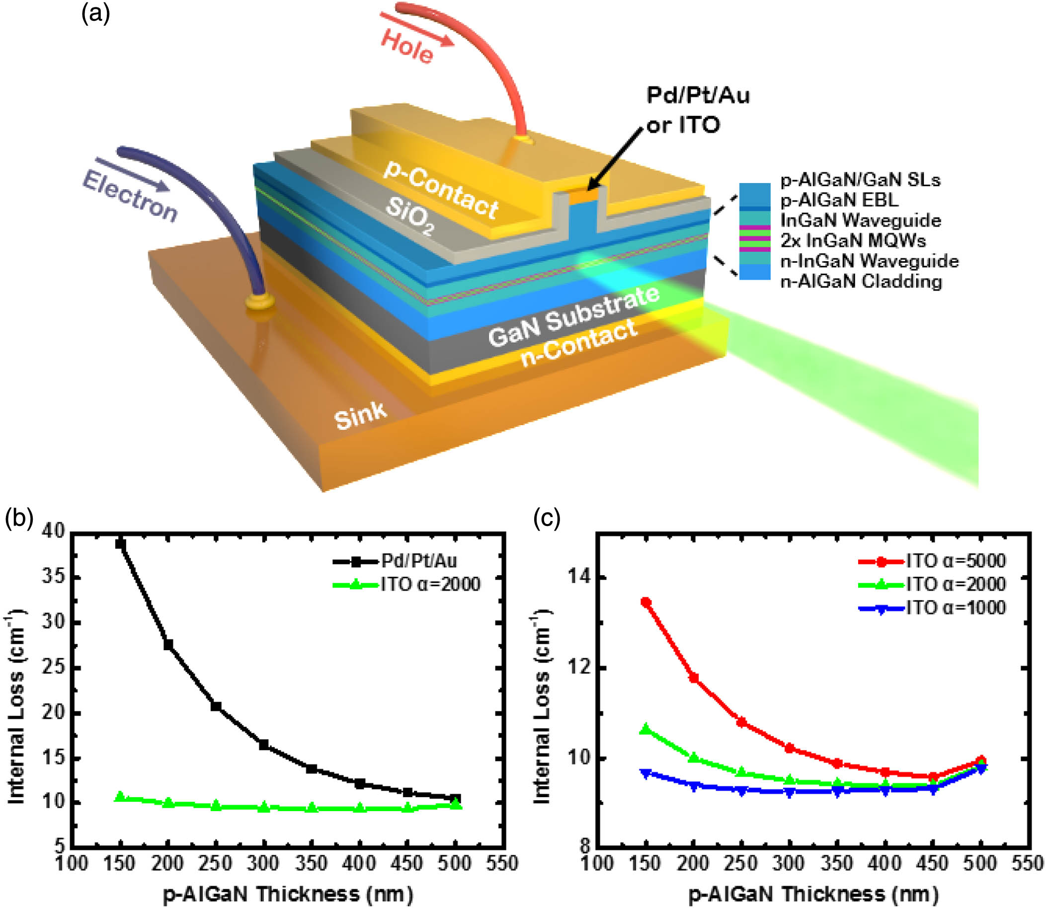
Green laser diodes (LDs) still perform worst among the visible and near-infrared spectrum range, which is called the “green gap.” Poor performance of green LDs is mainly related to the p-type AlGaN cladding layer, which on one hand imposes large thermal budget on InGaN quantum wells (QWs) during epitaxial growth, and on the other hand has poor electrical property especially when low growth temperature has to be used. We demonstrate in this work that a hybrid LD structure with an indium tin oxide (ITO) p-cladding layer can achieve threshold current density as low as , which is only one third of that of the conventional LD structure. The improvement is attributed to two benefits that are enabled by the ITO cladding layer. One is the reduced thermal budget imposed on QWs by reducing p-AlGaN layer thickness, and the other is the increasing hole concentration since a low Al content p-AlGaN cladding layer can be used in hybrid LD structures. Moreover, the slope efficiency is increased by 25% and the operation voltage is reduced by 0.6 V for hybrid green LDs. As a result, a 400 mW high-power green LD has been obtained. These results indicate that a hybrid LD structure can pave the way toward high-performance green LDs.
Photonics Research
2020, 8(3): 03000279


